Integrated NanoMaterial Lab
California NanoSystems Institute (CNSI)

Overview
The Integrated Nanomaterials Laboratory (INML) is a state-of-the-art nanomaterials synthesis and characterization facility. INML addresses the critical technological needs of the future through material development as we integrate nanoscience with disciplines such as electronics, photonics, renewable energy, chemistry, biology, and physics. the extensive technological advances made by the INML particularly in the areas of integrated iii-Sb/CMOS optoelectronics, infra- red photonics, and electronics form the basis of a large number of our on-going partnerships and collaborations.
Leadership

Contact
Equipment
-
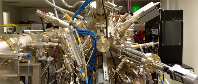
N-MBE system -
As/Sb-MBE system -
High-frequency probe station -
Cryogenic-Temperature Probe Station -
Broad-band Photoluminescence Characterization -
Micro-Photoluminescence Spectroscopy -
Cryogenic-Temperature Photoluminescence Spectroscopy -
FTIR Spectroscopy
Equipment
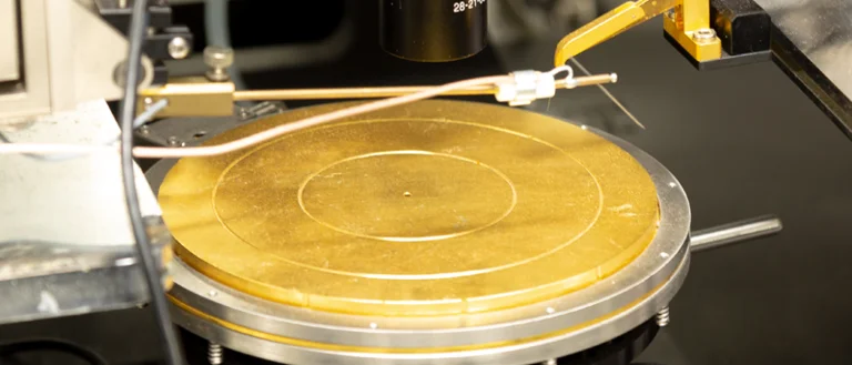
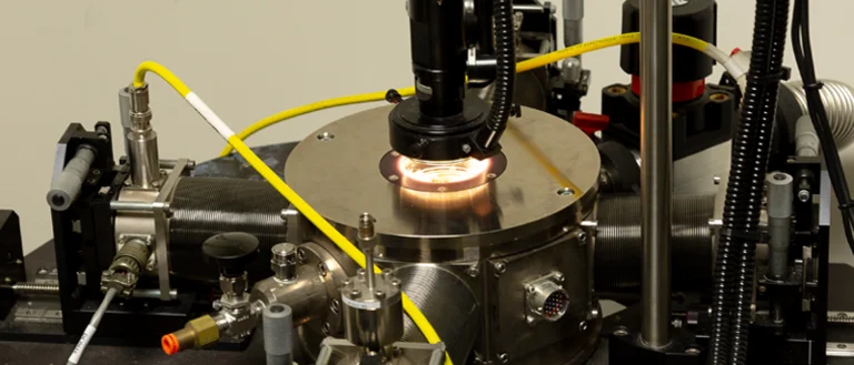
The N -MBE is designed for providing (In, Ga, Al) – N semiconductor wafer epitaxy services
- VEECO GEN-930 MBE
- In, Ga, Effusion cells, Al SUMO cells
- N plasma source with RF generator
- Fully automated N gas delivery system
- High temperature substrate heater (1200°C)
- Si, and Mg cells for doping
- Up to 3″ diameter wafers
- Growth control — MOLLY
- 100 a.mu. RGA
- RHEED and KSA400 software for in-situsurface monitoring and analysis
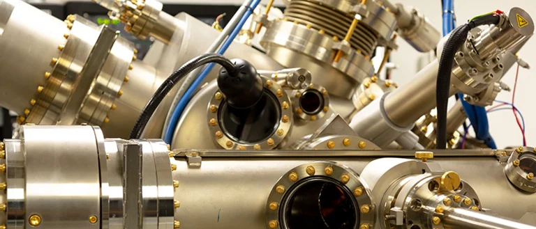
As/Sb-MBE system
The As/Sb -MBE is designed for providing (In, Ga, Al) / (As, Sb) semiconductor wafer epitaxy services
- VEECO GEN-930 MBE
- In, Ga, Al SUMO cells for group III
- Valved crackers for As and Sb cells
- Si, Te and Be cells for doping
- Up to 3″ diameter wafer holder
- Growth control — MOLLY
- 200 a.mu. RGA
- Optical pyrometer (440ºC – 800°C)
- RHEED for real time in-situmonitoring and KSA400 software for image/video capture for surface analysis
High-frequency probe station
For high frequency electronic and optoelectronic device characterization
- High Frequency (<50GHz)
- Full wavelength range laser available for photo-response measurement
- Integrated measurements (I-V, C-V, photoresponse)
Cryogenic-Temperature Probe Station
Lakeshore TTPX cryogenic-temperature probe station for device chips characterization before wire-bonding
- LN2 and LHe Temperature
- Integrated I-V & C-V measurements
- Agilent 4156C precision semiconductor parameter analyzer
- Agilent E4980A precision LCR meter, with frequency range from 20 hertz to 2 megahertz
- Fiber coupling laser beam for photo-response measurement
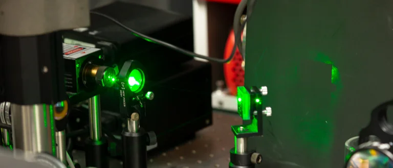
Broad-band Photoluminescence Characterization
For quick photoluminescence characterization at room temperature
- Acton SP2300 Spectrometer
- Multi-photodetectors available (Si, InGaAs, and Extended-InGaAs)
- Wavelength range: visible ~ 2.5 µm
- Excitation 200 mW, 532 nm, CW laser
- Operation: Room Temperature
- SR830 DSP Lock-in amplifier
- EG&G 7265 DSP Lock-in amplifier
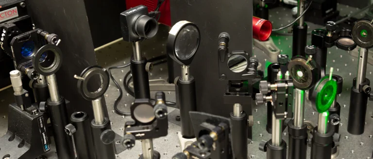
Micro-Photoluminescence Spectroscopy
Photoluminescence and time-resolved photoluminescence measurement in the near infrared wavelength (750nm-1600nm) for single nanostructure
- Princeton Instrument spectral 2D IR-CCD (750~1700nm)
- Acton SP2500 Spectrometer with triple gratings
- Excitation: 200mW 532nm CW laser
- Selective wavelength excitation (470nm~2000nm) by NKT super-continuum laser
- PL image function — 50x & 100x Plan Apo NIR objective lens (resolution <1 µm)
- Open-cycle JANIS and Oxford cryostat (4K or 77K)PicoHarp 300 TCSPC for time-resolved PL (visible-1650nm)
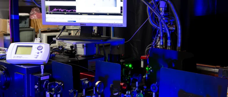
Cryogenic-Temperature Photoluminescence Spectroscopy
For temperature-dependent photoluminescence measurements (7K-300K)
- Acton SP2500 Spectrometer with triple gratings
- Excitation: 200 mW 532 nm CW laser
- Selective wavelength excitation (470nm~2000nm) by NKT super-continuum laser
- ARS closed-cycle cryostat (7K)
- Time-resolved PL (Visible-1700nm)
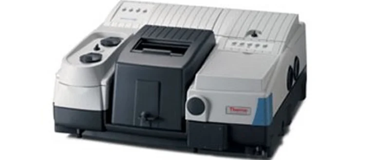
FTIR Spectroscopy
The FTIR spectroscopy system is designed for multi-functional infrared spectroscopy measurements (Photoluminescence, transmission, absorption, reflection)
- Thermo Scientific Nicolet 8700 FTIR
- Broad band detectors (InGaAs, InSb, MCT) to cover 800 nm ~ 10 µm
- External attachments for step-scan photoluminescence Integrated with JANIS ST-500 or Oxford LHe cryostats for cryogenic temperature measurements
- Integrated with Nicolet Continuum FT-IR microscope for down to mesa size characterization
- Combined with Parameter Analyzer and LCR meter for I-V & C-V measurements
N-MBE system
The N -MBE is designed for providing (In, Ga, Al) – N semiconductor wafer epitaxy services
- VEECO GEN-930 MBE
- In, Ga, Effusion cells, Al SUMO cells
- N plasma source with RF generator
- Fully automated N gas delivery system
- High temperature substrate heater (1200°C)
- Si, and Mg cells for doping
- Up to 3″ diameter wafers
- Growth control — MOLLY
- 100 a.mu. RGA
- RHEED and KSA400 software for in-situsurface monitoring and analysis
As/Sb-MBE system
The As/Sb -MBE is designed for providing (In, Ga, Al) / (As, Sb) semiconductor wafer epitaxy services
- VEECO GEN-930 MBE
- In, Ga, Al SUMO cells for group III
- Valved crackers for As and Sb cells
- Si, Te and Be cells for doping
- Up to 3″ diameter wafer holder
- Growth control — MOLLY
- 200 a.mu. RGA
- Optical pyrometer (440ºC – 800°C)
- RHEED for real time in-situmonitoring and KSA400 software for image/video capture for surface analysis